
24S+ LTC6804 BMS with various Sensors and Logging Function
A few weeks ago I decided to build a Battery Management System based on the LTC6804-1. The reason that made me build a BMS was the lack of economically priced high grade systems that are also customisable and extendable. The last few Battery Management Systems I used were also absolutely not serviceable (sealed with black epoxy and/or markings scraped off) and they were only usable for one chemistry. I want to have a little more control over my battery packs. Most importantly I want to have a cell logging function. So here’s a list of what my BMS can/will do (not all software features will be fully implemented. The hardware is working though):
- 16 Bit ADC reading resolution (I expect around 13-14Bit of accuracy)
- Balancing indicator led (balance current ~120mA)
- Easily customisable for different chemistries and cell numbers
- Daisy-chainable (Standard Version is 24S)
- Very low power consumption during standby
- No discharge current limit
- High charge current limit (20A+)
- Temperature and humidity sensor on the PCB
- Temperature sensor for the battery pack
- Altitude/Pressure sensor
- 3 Axis accelerometer
- Bluetooth interface
- RFID interface (supporting MIFARE and NFC)
- Throttle & Brake Input/Output
- SD Card slot for data logging
- Speedometer Input (via Hall or Reed)
- Buzzer
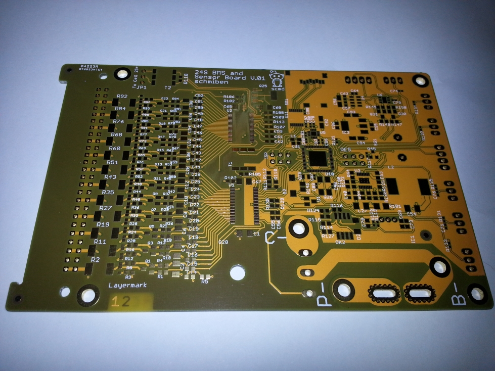
Well that’s quite a list… but I’m pretty sure it will grow with the next major Revision. I’m thinking about adding a display and some buttons and use a more powerful microcontroller. Depending on the project I certainly won’t assemble/use all of the features but it’s nice to have the option for additional features without redesigning the PCB. And since the sensors etc. don’t really use much space on the PCB they don’t add much to the cost. Due to the high pin count on certain components and the overall complexity I decided to design a 4-layer PCB rather than a 2-layer PCB. A 4-layer PCB also reduces the sesceptibility of EMI and generally improves the quality of the cell measurements if a solid ground plane is used. It’s certainly not hobbyist friendly to use multilayer boards and almost exclusively SMT components, but I really dislike THT components. They are bulky, less serviceable than SMT components and render much more effort assembling a PCB. In the case I decide to sell the BMS, I’d most certainly sell them with the SMT components preassembled.
The basic function
The brains of the BMS is an Atmega128A in the QFN-64 package. The LTC6804 is connected to the Atmega128A via the standard SPI interface which operates at 1Mhz. All following LTCs are connected via their isoSPI Port. When the BMS is in low power mode, the Atmega shuts down the secondary power source (DC/DC converter) and only draws a few microamperes from the first cell. All components except the Atmega and the LTC6804 are then completely shut down. This way the BMS won’t drain the battery when it’s not in use. If the BMS is in use the Atmega will power up the secondary power source, which supplies power to the rest of the components (max. 350mA). While in use, the BMS draws current from cells 1-12 and not only from cell 1. If the BMS is used in an electric vehicle, the throttle can be passed through the BMS and shut it down or reduce the power of the vehicle when a cell or the whole pack reaches a programmable low voltage threshold. There is also the possibility to connect a speed sensor to an interrupt pin of the Atmega. (Preferably a hall sensor from the motor). If a charger is connected to the battery, the BMS automatically wakes up und manages the charging and the balancing of the cells. After the battery is fully charged, the BMS disconnects the charger from the battery. When the BMS is active, either while charging or when the vehicle is turned on, the cell voltage and sensors can be read via bluetooth and the corresponding android app (which I probably won’t program myself). If an RFID Reader such as MFRC522 or PN532 is connected, it can be programmed as a keylock. Using the SD card interface, the sensor data can periodically be saved on a micro SD card.
Balancing algorithm
You may ask yourself if he’s already building his own BMS why the heck doens’t he use active balancing instead of passive balancing? Well the answer is quite simple: complexity. Although it would have been possible to implement active balancing I consider it to be an immense overkill. Active balancing is nice but its also very expensive in development. It is much harder to implement safe balancing/charge redistribution algorithms than just a “charge and cut off” algorithm. In addition, most battery packs stay fairly well in balance unless the cells are of very low quality. Since I don’t want to spend months developing intelligent algorithms I’m just going to use easily implementable algorithms. So far I haven’t decided wheter I will use the cell voltage based cut off method or actually balance the SOC.
First prototype and testing
Once again I ordered the PCBs at smart prototyping. This time I tried the yellow soldermask. In my opinion it looks quite ugly but that’s just my opinion. There’s a small disadvantage though: Because the soldermask is highly translucent it is hard to see wheter an area without tracks is covered or not. The spaces between the pads of the larger ICs -even the TSSOP14- are not covered by the soldermask. The next time I’m going to order red PCBs ^^.
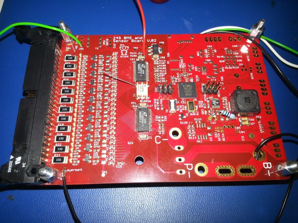
The size of the BMS is 130 x 83mm. With the connector plugged in it’s about 150 x 83mm. I dindn’t want to use the same connectors as most chinese BMS (the crappy EHR/XH/XHP) because crimping is just too time consuming and and I really think it’s a necessity to use connectors that won’t fall apart in a high vibration environment. The balancing connector is a 50 pin IDC lockable connector while all other signal connectors are WAGO type 733.
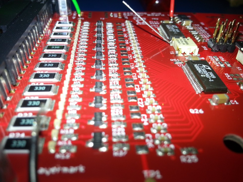
I left some tracks uncovered so I’ll be able to solder some wire on it. The current rating of the tracks would be too low for high current applications. 
The assembly took about 2 hours and went without any problems. Surprisingly, I had the whole thing except the second LTC6804 working within a couple of hours. I haven’t verified the measurements but they seemed to be quite accurate (less noise than a millivolt). The pressure/temperature/accelerometer and current sensor also gave plausible results. I havent tested the SD card and the buzzer but I already used those parts of the circuit successfully in another project. I didn’t test the charge FET at all but I don’t doubt it’s going to work.
After an hour of looking for the problem with the second LTC6804 in the software (it’s usually always the software 😛 ) I decided to have another look at the schematic. Soon the culprit was found. Two wires were connected incorrectly. Unfortunately the tracks of the corresponding wires are hardly accessible even thugh they are on the top layer of the board. Now I have to wait for the second revision. Because I only had very little time doing the revision I just corrected the error and changed a few package sizes for resistors and capacitors.
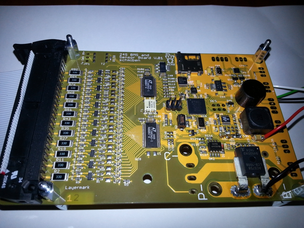
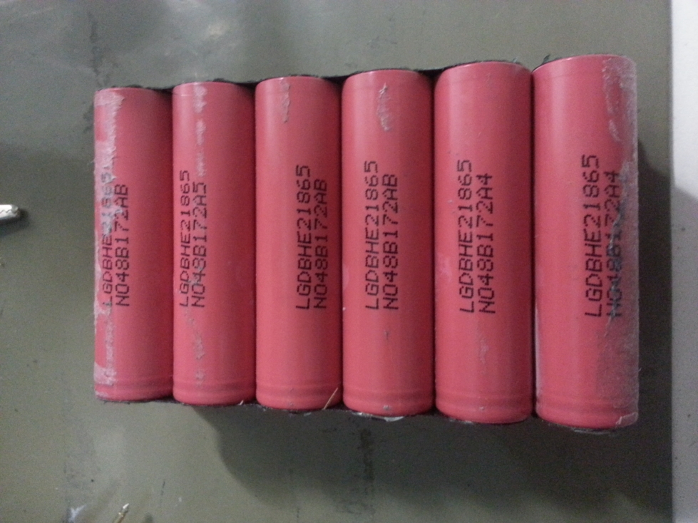
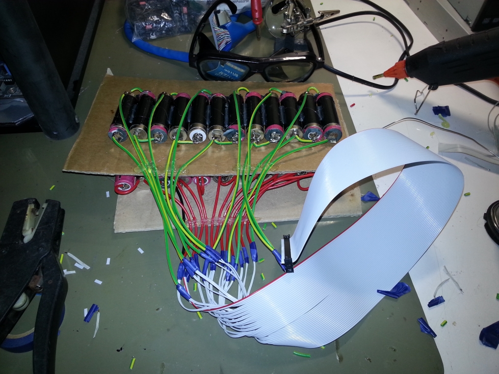
In order to test the BMS I built a small test rig with the two remaining packs of the Überbike project. It just a very quick and dirty (and dangerous) solution but it keeps up to the task.
Second prototype and testing
The new PCBs arrived a few days ago and I couldn’t wait to get it working. This time I only soldered the parts for necessary for voltage reading/balancing.
Unfortunately the second LTC still didn’t work altough the hardware seemed to be working. The second LTC6804 did actually respond. Let’s take a closer look at the signals. The trigger was set on the wake-up call.
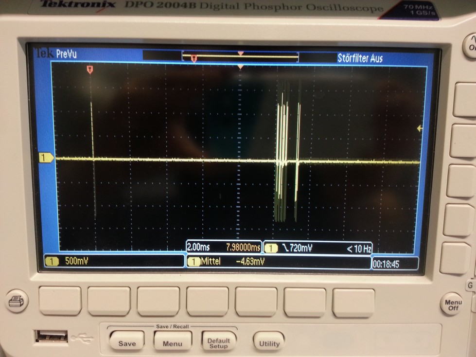
What do we have here? The pulses look like they interfere with each other. No wonder the LTCs don’t understand each other.
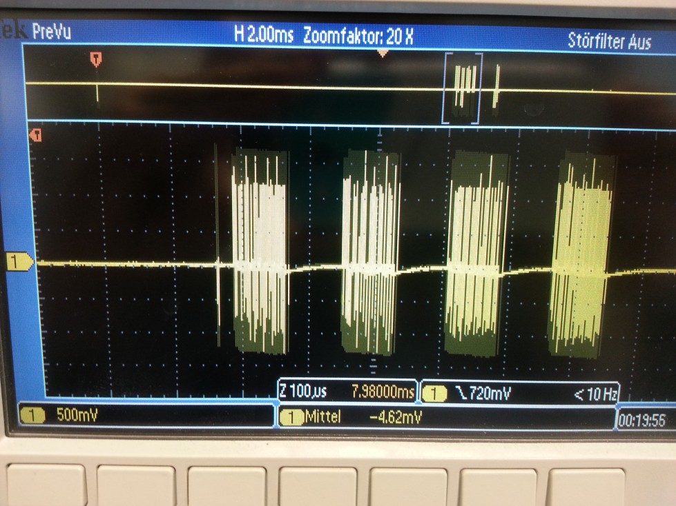
The single pulse looks quite clean but the rest is just gibberish.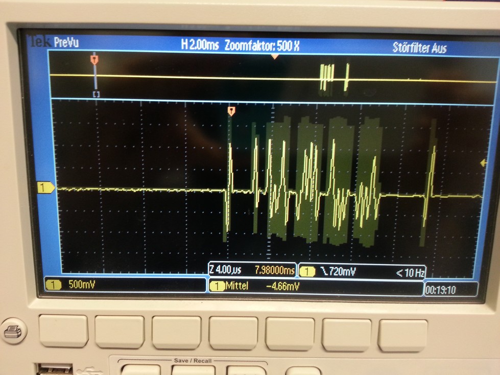
It looked like the LTCs couldn’t handle the speed. The isoSPI interface only allows a maximum clock frequency of 1MHz whereas the normal SPI interface seemed to work just fine with a clock speed of 4MHz. I didn’t capture the signals after fixing the problem.
The cell voltage readings are more or less accurate (1 mV difference compared to the SANWA PC5000a) but there’s still some room for improvement. The last cell shows a slightly too low value but I guess I already know where the problem is. I’ll keep you updated.
I am also currently working on a similar project. I got the demo board DC1942C, which is a demo board for LTC6804-2. I couldn’t get my board work. I am using an ARDUINO MEGA to communicate with the LTC6804-2 board. Can you please help me with my project?
Unfortunately not. I am currently not at home and don’t have any access to the related files and hardware. In order to get it to work with an Arduino you can just use their demo program. Linear Technology provides these files on the website. You will have to change some code in order to make it work. That’s all I can tell you righ now. Good luck
Hello
Will it be possible to buy from you the BMS system
No it won’t.
Hi,I am currently working with the similar project.May I ask you a question ;I am confused about LTC6804-1 programmable ability.I mean how ı can input registers to LTC with MPLAB or a similar program ,on Linear Technology’s webside there is a demo board and computer interface for it but is there any other way to programming LTC some way like microprocessors pickit etc.Because I want to create my own design,I don’t want to just use a already made system. I have been looking through the internet for it but there isn’t any satisfying answers for it. If you can answer my question ,I will be really glad.Thanks !
Hi there,
I suppose you need to study the datasheet a little bi more extensively. How do you program the registers? You simply send the corresponding SPI command. The commands are listed from p.46 of the datasheet. I would suggest that you take a look at the demo program on their website. Even if it’s written for Lin/Arduino you can use that code with some adaptions so you don’t have to deal with all the CRC stuff etc.. Cheers
Thanks for your answer,
I guess, I couldn’t express myself completely.I actually want to learn about which pins are the programming pins. As far as I understand from your reply I need to use the SPI communication. I was confused about that part because LTC have SPI,ısoSPI,I2C and GPIO pins for communication.Thanks for your time
And I forgot to write ,May I ask you about ; do I have to use LTCs recomended demoboard for programming I mean transfering my code from computer to LTC6804, or is there any other computer-LTC interface (like pic brenner) for programming. Thanks!
The programming pins are pin numbers 41-44 take the diagram in datasheet p.35 as a reference. If you connect two or more then you use the isoSPI to connect to other LTC’s. The LTC is not a microcontroller, you use a microcontroller to program the LTC via SPI and thats why you don’t need the demo board. Are you sure you really want to build everything from scratch? This project might be a little too ambitious.
I wasn’t only understand this part of LTC because I never work with a BMS chip before.Before this attempt I design a modular BMS with microcontrollers.Thanks for your reply.
Hi very nice project 😉 Is it possible to share your schematics because I’m going to make a similar project? Greetings from Austria
Honestly I would advise against using the LTC6804 in a new BMS project, it is one of the most delicate IC’s I’ve ever worked with. Especially during prototyping it’s a pain in the ass. It is possible to damage the IC halfway. That means the chip would still work, but return wrong levels of voltage on one cell. I would rather try something like the BQ76PL536A or BQ76PL455A. But to answer the question, no I’m not giving the schematics away but the whole schematic is basically in the datasheet anyway. Cheers from Brazil
Thank you for your fast reply and your advice! Do you have an idea how you damaged the IC halfway (ESD)? I just sampled the new generation chip LTC6811 for my project. Do you think that the problems still exist? The BQ76PL455A would indeed be an alternative so thanks for that hint and btw. no problem that you keep the schematics 😉
It must have been ESD, I can’t imagein a different cause. Even though I was working with a mat, ESD wristband, ESD soldering iron… You can try the newer version, they might have improved it. I would still go for the BQ from Texas. Why have they done so many revisions of that chip without any real improvements?
Hi very nice project Is it possible to share your schematics because I’m going to make a similar project?
Hi,
Can you send the component list and circuit. We have a electric vehicle project and we need to balance 20s battery.
Thank you,
Batuhan Yavaşoğlu
If you have read the comments before, you should already know the answer. Btw. it is easier to buy one than make it yourself. And if you have to make it yourself as a part of a university project, then do it yourself. This is the only way you’re going to learn how to design these circuits. Cheers
İs there any connetcion between first and second ltc6804?
Hi,
How are you doing? Hope you are doing fine. I know you have said in your previous post that you will not be giving your schematic. I don’t know if after all These time you have Change your mind. I am working on a Project with LTC6811 and I would like to know if you can help me with the schematic I would like to compare it with my model especially the passive balancing part.
Regards
Check your mail 😉
Hello, I work on BMS using two LTC6804-1 on same board. I’m stuck on SPI. Actually what I did not understand is how do we design the first IC’s V- pin? Should grounds of both IC’s be different? Could you please provide me your schematic? It is really important.
I am sorry you need to do your own homework, start with reading and trying to understand the datasheet. There are reference designs out there which exactly show the connections. On top of that, if you want help regarding SPI you should ask concise questions and provide info on your setup and what you have done so far. “I’m stuck” is a bit too vague.
Hi,
I designed a 20 cell system. I use a separate microprocessor for both ICs. I can see that the balance circuits of all cells are working in the arrangement I made on the code. However, the gate source voltage of the FETs I use in the balance circuits of the first 10 cells does not discharge. And I read the Vref1 voltage of the IC I used for the 10th and 20th in the range 0-120mV. Do you have any comments on these problems?
Thank you in advance.
Without the schematic I can’t make a qualified statement. What voltages do you get when you read the cell voltages? Are the upper ones correct and the lower ones not?
Lower ones are correct, upper ones read ~5.35 Voltage.
And you don’t get any CRC error when you read from the upper chip?
How do you provide isolation between two LTC6804s? Can you just give information about the IP and IM connections between the two LTCs? Could you just throw a schematic view of the communication of the two LTCs?
Hi Beni,
How are you doing? Hope you are doing well.
I have sent you a mail in your inbox. I would like to replace an LTC6803 with an LTC6812 in a schematic. Please can you have a look on it and let me know if I have done a proper modification?
Many thanks
Isso
Hello, I have been working with LTC6802 for more than 1 month. I made the configurations via STM32, but the LTC6802 IC draws more than 30 mA and is constantly variable. It does not pass by these values in the Datasheet. I think 6 LTC6802 burned due to ESD. I am developing bms for Electric Vehicle races. We have 1 month left. Can you help with the circuit diagram?
Well you haven’t provided any circuit diagram so it’s difficult to help… but yes the LTC is incredibly sensitive to ESD so you might be right on that one.
hello , ı am working on with 2 ltc6804-2 for 20S battery package how can ı use that without ltc6820 do u have any idea
No. Just read the datasheet…it says it the first page. you need to use LTC6804-1 for daisy chain.
Use the normal SPI on the first LTC and connect it to the second with isoSPI. The other option would be to use an isolated SPI driver…then you can use the LTC6804-2 but this might not make too much sense..
I have made a pcb with ltc6804-1 and it works perfectly fine with arduino, I cant interface them with Stm32, can you tell which are all the commands you called to read voltage,
Spi config :
115KBps,Msb first 8 bit mode